
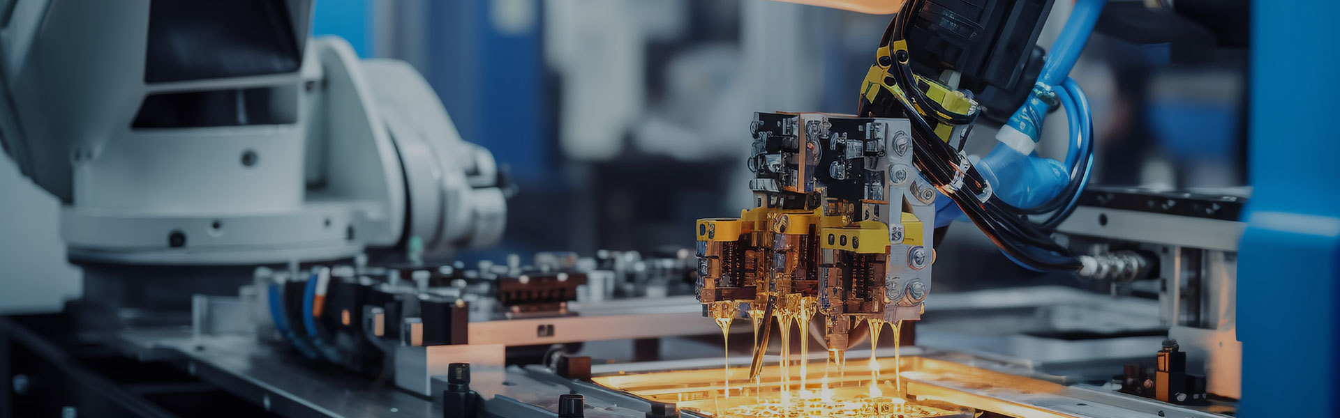
Unlocking the Potential of Deep Penetration Laser Welding Machines in Optoelectronics
Release time:
2026-07-18
Summary:
Deep penetration laser welding machines represent a significant advancement in the field of laser technology, particularly within the optoelectronics industry, where precision and efficiency are paramount. These machines employ high-energy laser beams capable of penetrating deep into materials, creating strong joints with minimal thermal distortion. This technology is increasingly being adopted fo
Deep penetration laser welding machines represent a significant advancement in the field of laser technology, particularly within the optoelectronics industry, where precision and efficiency are paramount. These machines employ high-energy laser beams capable of penetrating deep into materials, creating strong joints with minimal thermal distortion. This technology is increasingly being adopted for the welding of electronic components, including laser devices and their accessories, due to its numerous advantages.
One of the primary benefits of deep penetration laser welding is its ability to weld thicker materials with superior quality. Unlike traditional welding methods, which may struggle with thicker substrates, deep penetration laser welding can achieve a clean and robust weld seam even in challenging conditions. This capability is vital for manufacturers looking to ensure the structural integrity and longevity of their products, especially in applications where reliability is critical.
Another advantage is the precision it offers. The focused laser beam can be finely controlled, allowing for intricate designs and complex joint geometries that are often required in the fabrication of electronic devices. This accuracy minimizes the risk of defects and reduces the need for extensive post-weld processing, ultimately leading to a more efficient production cycle.
Furthermore, deep penetration laser welding is known for its speed. The high welding speed facilitates increased productivity, enabling manufacturers to meet growing market demands without compromising quality. Additionally, the non-contact nature of laser welding reduces the risk of contamination and ensures cleaner working conditions, which is essential in the sensitive environment of electronic component production.
In terms of versatility, deep penetration laser welding can be applied to a wide range of materials, including metals and certain plastics, making it an excellent choice for diverse applications within the optoelectronics field. Whether it's for the assembly of light guides, optical components, or housing for laser systems, this technology can adapt to various material combinations and thicknesses.
Moreover, the integration of deep penetration laser welding machines into manufacturing processes can enhance the sustainability of production. By reducing waste and energy consumption compared to traditional methods, these machines contribute to a greener manufacturing approach, aligning with the growing emphasis on environmental responsibility in the electronics industry.
In conclusion, deep penetration laser welding machines are revolutionizing the way electronic components are produced, offering exceptional quality, speed, and versatility. As the optoelectronics industry continues to evolve, embracing these advanced technologies will be crucial for manufacturers aiming to maintain a competitive edge while delivering high-quality products to the market.
One of the primary benefits of deep penetration laser welding is its ability to weld thicker materials with superior quality. Unlike traditional welding methods, which may struggle with thicker substrates, deep penetration laser welding can achieve a clean and robust weld seam even in challenging conditions. This capability is vital for manufacturers looking to ensure the structural integrity and longevity of their products, especially in applications where reliability is critical.
Another advantage is the precision it offers. The focused laser beam can be finely controlled, allowing for intricate designs and complex joint geometries that are often required in the fabrication of electronic devices. This accuracy minimizes the risk of defects and reduces the need for extensive post-weld processing, ultimately leading to a more efficient production cycle.
Furthermore, deep penetration laser welding is known for its speed. The high welding speed facilitates increased productivity, enabling manufacturers to meet growing market demands without compromising quality. Additionally, the non-contact nature of laser welding reduces the risk of contamination and ensures cleaner working conditions, which is essential in the sensitive environment of electronic component production.
In terms of versatility, deep penetration laser welding can be applied to a wide range of materials, including metals and certain plastics, making it an excellent choice for diverse applications within the optoelectronics field. Whether it's for the assembly of light guides, optical components, or housing for laser systems, this technology can adapt to various material combinations and thicknesses.
Moreover, the integration of deep penetration laser welding machines into manufacturing processes can enhance the sustainability of production. By reducing waste and energy consumption compared to traditional methods, these machines contribute to a greener manufacturing approach, aligning with the growing emphasis on environmental responsibility in the electronics industry.
In conclusion, deep penetration laser welding machines are revolutionizing the way electronic components are produced, offering exceptional quality, speed, and versatility. As the optoelectronics industry continues to evolve, embracing these advanced technologies will be crucial for manufacturers aiming to maintain a competitive edge while delivering high-quality products to the market.
Previous Page
Previous Page
Real-time information




Copyright©2024 Shandong Haihai Laser Technology Co., Ltd.